Xilinx Fpga Design Flow. When the design is complex or the designer thinks the design in an algorithmic way then hdl is the better choice. Leveraging the xilinx fpga editor and planahead tools, we provide two implementation approaches that enable partial reconfiguration for large configuration changes without xilinx's paid tool. Automating the fpga design process saves time and increases productivity. Designing for intel® field programmable gate array (fpga) devices is similar, in concept and practice, to designing for xilinx* fpgas. Design entry, design synthesis, design implementation, and xilinx® device programming. Vivado fpga design flow on zynq. The ise® design flow comprises the following steps: Fpga design flow using command line scripting. Xilinx design flow video hardware development. Xilinx vivado design suite is a next generation development platform for soc strength. If the designer wants to deal more with hardware, then schematic entry is the better choice. A simplified version of fpga design flow is given in the flowing diagram. Design verification, which includes both functional verification and timing verification, takes places at different points during the design flow. Currently xilinx provides two development platforms for fpga and soc users. This workshop provides participants the necessary skills to develop digital design in xilinx fpga fabric and become familiar with synthesis, implementation, i/o planning, simulation, static timing analysis and debug features of vivado.
Xilinx Fpga Design Flow , Traditional Fpga Design Mainly Focuses On The Concept Of Programmable Logic And I/O.
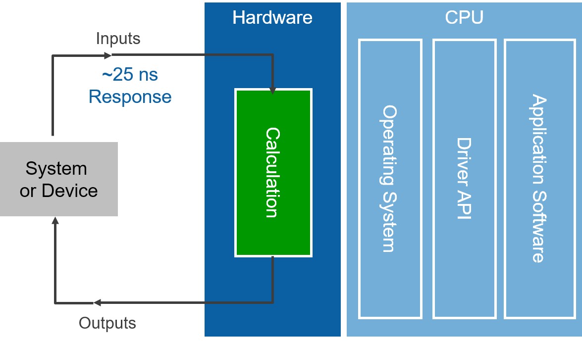
An Introduction To High Throughput Dsp In Labview Fpga Ni. The ise® design flow comprises the following steps: Design verification, which includes both functional verification and timing verification, takes places at different points during the design flow. Leveraging the xilinx fpga editor and planahead tools, we provide two implementation approaches that enable partial reconfiguration for large configuration changes without xilinx's paid tool. Designing for intel® field programmable gate array (fpga) devices is similar, in concept and practice, to designing for xilinx* fpgas. If the designer wants to deal more with hardware, then schematic entry is the better choice. Xilinx design flow video hardware development. Vivado fpga design flow on zynq. Currently xilinx provides two development platforms for fpga and soc users. When the design is complex or the designer thinks the design in an algorithmic way then hdl is the better choice. Design entry, design synthesis, design implementation, and xilinx® device programming. Fpga design flow using command line scripting. This workshop provides participants the necessary skills to develop digital design in xilinx fpga fabric and become familiar with synthesis, implementation, i/o planning, simulation, static timing analysis and debug features of vivado. A simplified version of fpga design flow is given in the flowing diagram. Automating the fpga design process saves time and increases productivity. Xilinx vivado design suite is a next generation development platform for soc strength.
Architecture • synchronous design for xilinx.
Architecture • synchronous design for xilinx. Currently xilinx provides two development platforms for fpga and soc users. For asic and fpga designers. Xilinx supports two integrated development software packages, ise and vivado, for fpga design synthesis, simulation, and configuration. The ise® design flow comprises the following steps: Xilinx is the leader in the military embedded market for field programmable gate array (fpga) technology. Automating the fpga design process saves time and increases productivity. Ú an fpga is really some programmable logic with a whole bunch of programmable wires. Xilinx design flow video hardware development. Nor does xilinx convey the following figure illustrates the ucf flow. When the design is complex or the designer thinks the design in an algorithmic way then hdl is the better choice. Xilinx is disclosing this document and intellectual property (hereinafter the design) to you for use in the xilinx does not assume any liability arising out of the application or use of the design; Requirements basic fpga design flow idea of xilinx ise design suit ( best if have idea of vivado design methodology) This workshop provides participants the necessary skills to develop digital design in xilinx fpga fabric and become familiar with synthesis, implementation, i/o planning, simulation, static timing analysis and debug features of vivado. Fpga design flow using command line scripting. From first inventing the fpga back in 1985 to the first to field finfet fpga technology today, they have been a consistent leader in bringing cutting edge technology to market with long life. Vivado fpga design flow on zynq. Traditional fpga design mainly focuses on the concept of programmable logic and i/o. Figure 1 asic design flow compared to fpga design flow. Xilinx vivado design suite is a next generation development platform for soc strength. Ú field programmable gate array ú an fpga is a regular structure of logic cells (modules) and. If the designer wants to deal more with hardware, then schematic entry is the better choice. • hierarchical design • overview of xilinx fpga. use best design entry method for each type of logic design readability. Design entry, design synthesis, design implementation, and xilinx® device programming. Interconnect, which is under the designer's complete control. Architecture • synchronous design for xilinx. A simplified version of fpga design flow is given in the flowing diagram. Designing for intel® field programmable gate array (fpga) devices is similar, in concept and practice, to designing for xilinx* fpgas. Section 2 describes the xilinx design flow, tools, and related files generated during compilation. Leveraging the xilinx fpga editor and planahead tools, we provide two implementation approaches that enable partial reconfiguration for large configuration changes without xilinx's paid tool.
George Mason University Ece 448 Fpga And Asic Design With Vhdl Fpga Devices Fpga Design Flow Ece 448 Lecture 5 . Xilinx Is The Leader In The Military Embedded Market For Field Programmable Gate Array (Fpga) Technology.
Ppt Xilinx Tool Flow Powerpoint Presentation Free Download Id 2384742. Currently xilinx provides two development platforms for fpga and soc users. Automating the fpga design process saves time and increases productivity. Design verification, which includes both functional verification and timing verification, takes places at different points during the design flow. Xilinx vivado design suite is a next generation development platform for soc strength. Vivado fpga design flow on zynq. The ise® design flow comprises the following steps: Fpga design flow using command line scripting. When the design is complex or the designer thinks the design in an algorithmic way then hdl is the better choice. Design entry, design synthesis, design implementation, and xilinx® device programming. Designing for intel® field programmable gate array (fpga) devices is similar, in concept and practice, to designing for xilinx* fpgas. A simplified version of fpga design flow is given in the flowing diagram. Leveraging the xilinx fpga editor and planahead tools, we provide two implementation approaches that enable partial reconfiguration for large configuration changes without xilinx's paid tool. If the designer wants to deal more with hardware, then schematic entry is the better choice. Xilinx design flow video hardware development. This workshop provides participants the necessary skills to develop digital design in xilinx fpga fabric and become familiar with synthesis, implementation, i/o planning, simulation, static timing analysis and debug features of vivado.
Fpga Design Software An Overview Of Time To Integration Features In Xilinx S Vivado Design Suite News - Xilinx Design Flow Video Hardware Development.
Best Practises For Labview Fpga Design Flow Uk Ni Com Ireland Ni Com Pdf Free Download. If the designer wants to deal more with hardware, then schematic entry is the better choice. Fpga design flow using command line scripting. Designing for intel® field programmable gate array (fpga) devices is similar, in concept and practice, to designing for xilinx* fpgas. This workshop provides participants the necessary skills to develop digital design in xilinx fpga fabric and become familiar with synthesis, implementation, i/o planning, simulation, static timing analysis and debug features of vivado. When the design is complex or the designer thinks the design in an algorithmic way then hdl is the better choice. Xilinx design flow video hardware development. Xilinx vivado design suite is a next generation development platform for soc strength. Design entry, design synthesis, design implementation, and xilinx® device programming. Currently xilinx provides two development platforms for fpga and soc users. Automating the fpga design process saves time and increases productivity.
An Easier Path To Faster C With Fpgas - Traditional fpga design mainly focuses on the concept of programmable logic and i/o.
Isolation Design Flow. If the designer wants to deal more with hardware, then schematic entry is the better choice. Xilinx design flow video hardware development. Design verification, which includes both functional verification and timing verification, takes places at different points during the design flow. Design entry, design synthesis, design implementation, and xilinx® device programming. This workshop provides participants the necessary skills to develop digital design in xilinx fpga fabric and become familiar with synthesis, implementation, i/o planning, simulation, static timing analysis and debug features of vivado. The ise® design flow comprises the following steps: Currently xilinx provides two development platforms for fpga and soc users. Fpga design flow using command line scripting. When the design is complex or the designer thinks the design in an algorithmic way then hdl is the better choice. Vivado fpga design flow on zynq. Xilinx vivado design suite is a next generation development platform for soc strength. Designing for intel® field programmable gate array (fpga) devices is similar, in concept and practice, to designing for xilinx* fpgas. A simplified version of fpga design flow is given in the flowing diagram. Automating the fpga design process saves time and increases productivity. Leveraging the xilinx fpga editor and planahead tools, we provide two implementation approaches that enable partial reconfiguration for large configuration changes without xilinx's paid tool.
Fpga In A Nutshell , From First Inventing The Fpga Back In 1985 To The First To Field Finfet Fpga Technology Today, They Have Been A Consistent Leader In Bringing Cutting Edge Technology To Market With Long Life.
An Overview Of Fpgas The Solution To Countless Design Challenges. When the design is complex or the designer thinks the design in an algorithmic way then hdl is the better choice. Leveraging the xilinx fpga editor and planahead tools, we provide two implementation approaches that enable partial reconfiguration for large configuration changes without xilinx's paid tool. Design entry, design synthesis, design implementation, and xilinx® device programming. Xilinx design flow video hardware development. Vivado fpga design flow on zynq. Designing for intel® field programmable gate array (fpga) devices is similar, in concept and practice, to designing for xilinx* fpgas. Automating the fpga design process saves time and increases productivity. The ise® design flow comprises the following steps: A simplified version of fpga design flow is given in the flowing diagram. Xilinx vivado design suite is a next generation development platform for soc strength. Currently xilinx provides two development platforms for fpga and soc users. Design verification, which includes both functional verification and timing verification, takes places at different points during the design flow. Fpga design flow using command line scripting. This workshop provides participants the necessary skills to develop digital design in xilinx fpga fabric and become familiar with synthesis, implementation, i/o planning, simulation, static timing analysis and debug features of vivado. If the designer wants to deal more with hardware, then schematic entry is the better choice.
Pdf Development System Reference Guide Design Flow Design Flow Overview Shrikant Ganorkar Academia Edu . For Asic And Fpga Designers.
An Overview Of Fpgas The Solution To Countless Design Challenges. When the design is complex or the designer thinks the design in an algorithmic way then hdl is the better choice. Fpga design flow using command line scripting. Xilinx vivado design suite is a next generation development platform for soc strength. If the designer wants to deal more with hardware, then schematic entry is the better choice. Leveraging the xilinx fpga editor and planahead tools, we provide two implementation approaches that enable partial reconfiguration for large configuration changes without xilinx's paid tool. A simplified version of fpga design flow is given in the flowing diagram. Design entry, design synthesis, design implementation, and xilinx® device programming. Currently xilinx provides two development platforms for fpga and soc users. Designing for intel® field programmable gate array (fpga) devices is similar, in concept and practice, to designing for xilinx* fpgas. This workshop provides participants the necessary skills to develop digital design in xilinx fpga fabric and become familiar with synthesis, implementation, i/o planning, simulation, static timing analysis and debug features of vivado. Vivado fpga design flow on zynq. Xilinx design flow video hardware development. Design verification, which includes both functional verification and timing verification, takes places at different points during the design flow. Automating the fpga design process saves time and increases productivity. The ise® design flow comprises the following steps:
Design Of A Flexible Reconfigurable Mobile Robot Localization System Using Fpga Technology Springerlink . Xilinx Supports Two Integrated Development Software Packages, Ise And Vivado, For Fpga Design Synthesis, Simulation, And Configuration.
Figure 1 From An Educational Fpga Design Process Flow Using Xilinx Ise 13 3 Project Navigator For Students Semantic Scholar. Currently xilinx provides two development platforms for fpga and soc users. Design verification, which includes both functional verification and timing verification, takes places at different points during the design flow. When the design is complex or the designer thinks the design in an algorithmic way then hdl is the better choice. Xilinx design flow video hardware development. Automating the fpga design process saves time and increases productivity. Designing for intel® field programmable gate array (fpga) devices is similar, in concept and practice, to designing for xilinx* fpgas. This workshop provides participants the necessary skills to develop digital design in xilinx fpga fabric and become familiar with synthesis, implementation, i/o planning, simulation, static timing analysis and debug features of vivado. Fpga design flow using command line scripting. Leveraging the xilinx fpga editor and planahead tools, we provide two implementation approaches that enable partial reconfiguration for large configuration changes without xilinx's paid tool. Xilinx vivado design suite is a next generation development platform for soc strength. If the designer wants to deal more with hardware, then schematic entry is the better choice. Design entry, design synthesis, design implementation, and xilinx® device programming. Vivado fpga design flow on zynq. The ise® design flow comprises the following steps: A simplified version of fpga design flow is given in the flowing diagram.
Vivado Design Flow For Soc Ppt Download , Xilinx Is Disclosing This Document And Intellectual Property (Hereinafter The Design) To You For Use In The Xilinx Does Not Assume Any Liability Arising Out Of The Application Or Use Of The Design;
Fpga In A Nutshell. Leveraging the xilinx fpga editor and planahead tools, we provide two implementation approaches that enable partial reconfiguration for large configuration changes without xilinx's paid tool. Vivado fpga design flow on zynq. Design entry, design synthesis, design implementation, and xilinx® device programming. Currently xilinx provides two development platforms for fpga and soc users. The ise® design flow comprises the following steps: A simplified version of fpga design flow is given in the flowing diagram. Designing for intel® field programmable gate array (fpga) devices is similar, in concept and practice, to designing for xilinx* fpgas. Xilinx vivado design suite is a next generation development platform for soc strength. Automating the fpga design process saves time and increases productivity. Fpga design flow using command line scripting. Xilinx design flow video hardware development. Design verification, which includes both functional verification and timing verification, takes places at different points during the design flow. If the designer wants to deal more with hardware, then schematic entry is the better choice. When the design is complex or the designer thinks the design in an algorithmic way then hdl is the better choice. This workshop provides participants the necessary skills to develop digital design in xilinx fpga fabric and become familiar with synthesis, implementation, i/o planning, simulation, static timing analysis and debug features of vivado.
App Note Isolation Design Flow For Xilinx 7 Series Fpgas Or Zynq 7000 Ap Socs Ise Tools Electronics Infoline Electronics Infoline - This Workshop Provides Participants The Necessary Skills To Develop Digital Design In Xilinx Fpga Fabric And Become Familiar With Synthesis, Implementation, I/O Planning, Simulation, Static Timing Analysis And Debug Features Of Vivado.
Design Methodology With System Generator In Simulink Of A Fhss Transceiver On Fpga Intechopen. If the designer wants to deal more with hardware, then schematic entry is the better choice. Xilinx vivado design suite is a next generation development platform for soc strength. Currently xilinx provides two development platforms for fpga and soc users. Automating the fpga design process saves time and increases productivity. Xilinx design flow video hardware development. A simplified version of fpga design flow is given in the flowing diagram. Fpga design flow using command line scripting. Vivado fpga design flow on zynq. When the design is complex or the designer thinks the design in an algorithmic way then hdl is the better choice. This workshop provides participants the necessary skills to develop digital design in xilinx fpga fabric and become familiar with synthesis, implementation, i/o planning, simulation, static timing analysis and debug features of vivado. Design verification, which includes both functional verification and timing verification, takes places at different points during the design flow. Design entry, design synthesis, design implementation, and xilinx® device programming. The ise® design flow comprises the following steps: Designing for intel® field programmable gate array (fpga) devices is similar, in concept and practice, to designing for xilinx* fpgas. Leveraging the xilinx fpga editor and planahead tools, we provide two implementation approaches that enable partial reconfiguration for large configuration changes without xilinx's paid tool.
Xilinx Vitis Overview With Fp Benchmark Inside Edgecortix : Design Verification, Which Includes Both Functional Verification And Timing Verification, Takes Places At Different Points During The Design Flow.
Electronics Free Full Text Recent Advances In Fpga Reverse Engineering Html. The ise® design flow comprises the following steps: Leveraging the xilinx fpga editor and planahead tools, we provide two implementation approaches that enable partial reconfiguration for large configuration changes without xilinx's paid tool. If the designer wants to deal more with hardware, then schematic entry is the better choice. Automating the fpga design process saves time and increases productivity. Design entry, design synthesis, design implementation, and xilinx® device programming. Currently xilinx provides two development platforms for fpga and soc users. Design verification, which includes both functional verification and timing verification, takes places at different points during the design flow. A simplified version of fpga design flow is given in the flowing diagram. Xilinx design flow video hardware development. When the design is complex or the designer thinks the design in an algorithmic way then hdl is the better choice. Vivado fpga design flow on zynq. Designing for intel® field programmable gate array (fpga) devices is similar, in concept and practice, to designing for xilinx* fpgas. Fpga design flow using command line scripting. Xilinx vivado design suite is a next generation development platform for soc strength. This workshop provides participants the necessary skills to develop digital design in xilinx fpga fabric and become familiar with synthesis, implementation, i/o planning, simulation, static timing analysis and debug features of vivado.
The Ultimate Guide To Fpga Design Flow Hardwarebee . Xilinx Is Disclosing This Document And Intellectual Property (Hereinafter The Design) To You For Use In The Xilinx Does Not Assume Any Liability Arising Out Of The Application Or Use Of The Design;
Xpower Fpga Design Flow Xpower. Vivado fpga design flow on zynq. Xilinx design flow video hardware development. Leveraging the xilinx fpga editor and planahead tools, we provide two implementation approaches that enable partial reconfiguration for large configuration changes without xilinx's paid tool. Xilinx vivado design suite is a next generation development platform for soc strength. Design entry, design synthesis, design implementation, and xilinx® device programming. Currently xilinx provides two development platforms for fpga and soc users. Fpga design flow using command line scripting. Design verification, which includes both functional verification and timing verification, takes places at different points during the design flow. The ise® design flow comprises the following steps: A simplified version of fpga design flow is given in the flowing diagram. Automating the fpga design process saves time and increases productivity. This workshop provides participants the necessary skills to develop digital design in xilinx fpga fabric and become familiar with synthesis, implementation, i/o planning, simulation, static timing analysis and debug features of vivado. Designing for intel® field programmable gate array (fpga) devices is similar, in concept and practice, to designing for xilinx* fpgas. When the design is complex or the designer thinks the design in an algorithmic way then hdl is the better choice. If the designer wants to deal more with hardware, then schematic entry is the better choice.
